If you've spent any time learning about GPU performance, you've probably heard people say that memory is the bottleneck.
In fact, in the previous article we showed that during LLM decoding, an NVIDIA H100 spends far more time moving model weights from memory than performing the actual computations.
If memory is the bottleneck, the obvious question becomes:
Why doesn't the GPU just have one very large, very fast memory?
The answer is simple.
Large memories are slow.
Fast memories are small.
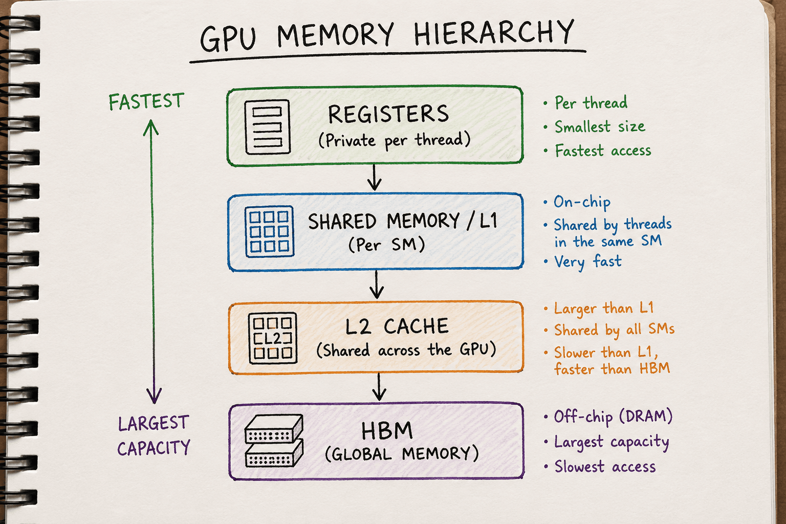
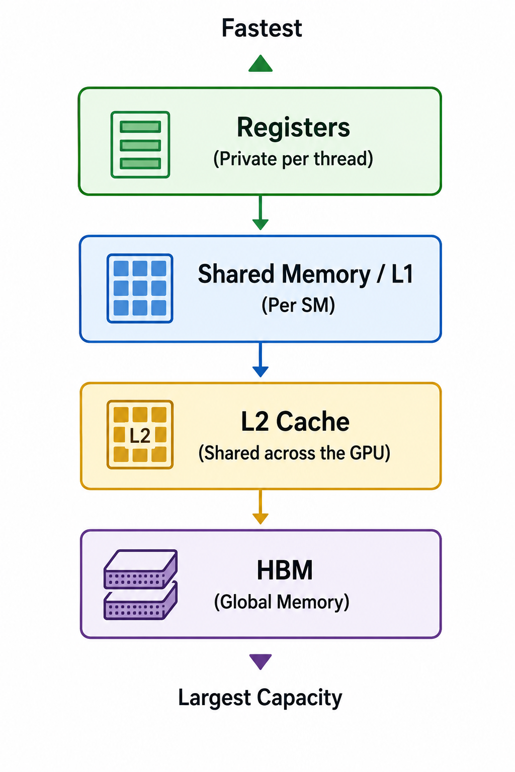
Modern GPUs solve this problem by organising memory into different levels, each with its own speed, capacity and purpose. This organisation is known as the GPU memory hierarchy.
Each level is designed to balance three competing goals:
- Capacity
- Speed
- Cost
As memory gets closer to the compute units, it becomes much faster but also much smaller.
As it moves further away, it becomes much larger but also much slower to access.
Understanding this hierarchy is one of the most important steps in understanding GPU performance because every computation depends on moving data through it.
Throughout this article we'll use the NVIDIA H100 SXM5 as our reference GPU.
Although the exact numbers differ between GPU generations, the overall memory hierarchy is very similar across modern NVIDIA GPUs.
The GPU Memory Hierarchy
At a high level, GPU memory can be divided into two broad categories.
On-chip memory
On-chip memory is physically located on the same silicon die as the Streaming Multiprocessors (SMs), CUDA Cores and Tensor Cores.
Because this memory is so close to the compute units, it has very low latency and extremely high bandwidth.
The trade-off is capacity.
There simply isn't enough space on the silicon die to build hundreds of gigabytes of on-chip memory, so these memories are intentionally kept small.
The on-chip memories we'll cover are:
- Registers
- Shared Memory / L1 Cache
Off-chip memory
Off-chip memory sits outside the GPU die.
Although it's much further away from the compute units, it can provide vastly more storage capacity.
This includes:
- L2 Cache
- HBM (Global Memory)
This movement of data is often the largest contributor to GPU execution time.
We'll now look at each level, starting with the memory that's closest to the compute units.
1. Registers
Registers are the first stop in the GPU memory hierarchy.
If you've ever wondered where a thread stores the values it's currently working on, the answer is registers.
Registers are tiny pieces of memory located inside each Streaming Multiprocessor (SM), sitting directly beside the CUDA Cores and Tensor Cores. Because they are so close to the compute units, they are the fastest memory available on the GPU.
Accessing a register typically takes only one clock cycle, making it several orders of magnitude faster than reading data from HBM.
Every Thread Has Its Own Registers
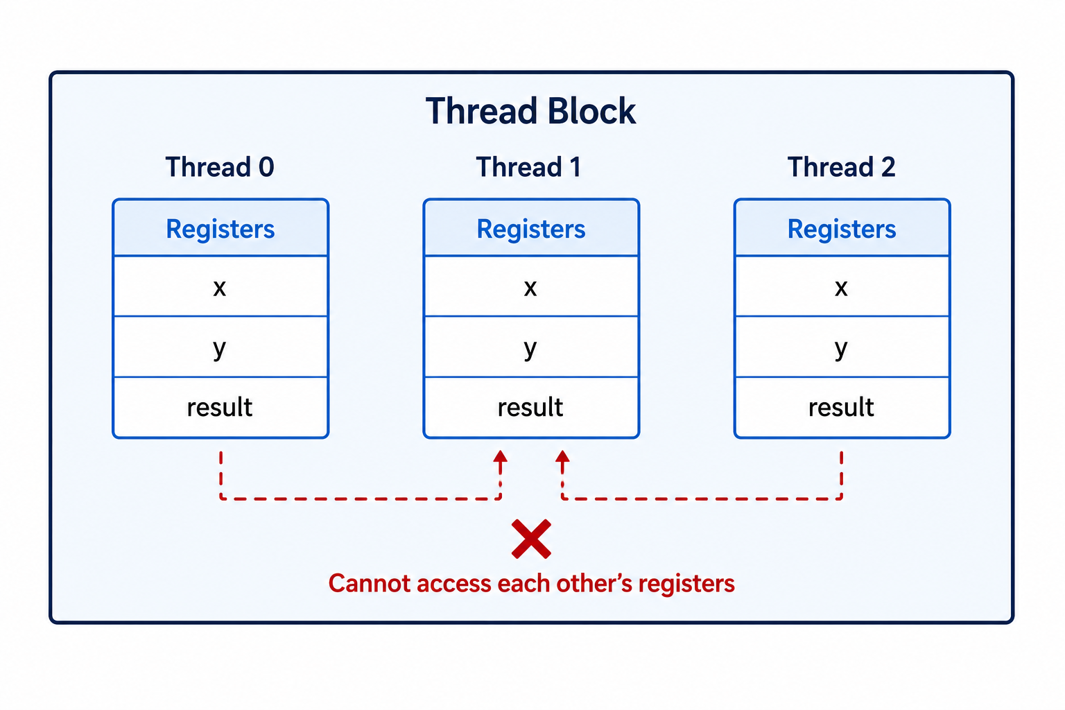
Unlike shared memory, registers are private to each thread.
If a kernel launches one million threads, each of those threads receives its own set of registers.
No other thread can read or modify them.
For example, consider this simple CUDA code:
__global__ void add(float* A, float* B, float* C) {
    int i = threadIdx.x;

    float x = A[i];
    float y = B[i];

    float result = x + y;

    C[i] = result;
}
For every thread, values such as i, x, y and result are typically stored in registers while the thread is executing.
Each thread has its own copy.
If Thread 0 changes the value of result, Thread 1 cannot see it because their registers are completely independent.
This isolation allows millions of threads to execute simultaneously without interfering with one another.
How Many Registers Does an H100 Have?
Each SM on an NVIDIA H100 contains:
65,536 registers

Each register stores 32 bits, or 4 bytes.

That means the total register capacity per SM is:

65,536 × 4 bytes

= 262,144 bytes

= 256 KB
The H100 SXM5 contains 132 Streaming Multiprocessors, so the total register capacity across the GPU is:
132 × 256 KB

= 33,792 KB

≈ 33 MB
Although 33 MB might sound small compared to 80 GB of HBM, remember that registers are designed for speed, not capacity.
They only store the values that threads are actively using at that moment.
Why Registers Matter
Every calculation performed by a thread depends on registers.
When the Tensor Cores or CUDA Cores perform an operation, the operands are read from registers, and the result is usually written back into another register before being used again or eventually written to global memory.
The closer the data stays to the compute units, the faster the GPU can execute instructions.
This is why the compiler tries to keep as many variables as possible in registers.
What Happens When There Aren't Enough Registers?
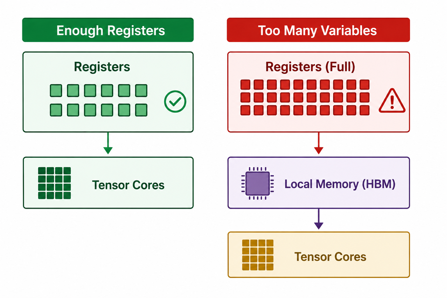
Registers are limited.
Every thread consumes some number of registers, and the total number of registers available on an SM is fixed.
If a kernel requires more registers than are available, the compiler has no choice but to place the excess variables somewhere else.
This process is known as register spilling.
When register spilling occurs, the extra variables are stored in local memory instead.
Despite its name, local memory is not located on-chip.
It lives in the GPU's HBM, which is hundreds of clock cycles away from the compute units.
That means every spilled variable now requires a much slower memory access.
This can significantly reduce kernel performance.
We'll look at local memory later in this article, but for now it's enough to remember one simple rule:
The more data a thread can keep in registers, the better.
2. Shared Memory and L1 Cache
The next level in the GPU memory hierarchy is Shared Memory and L1 Cache.
Like registers, they are located on-chip, meaning they sit inside each Streaming Multiprocessor (SM) very close to the CUDA and Tensor Cores.
Because they are on-chip, they are much faster than accessing HBM, typically taking around 20–30 clock cycles instead of hundreds.
Although you'll often hear people talk about Shared Memory and L1 Cache as if they are separate memories, modern NVIDIA GPUs combine them into the same pool of SRAM.
On an NVIDIA H100, each SM contains:
256 KB of on-chip SRAM
This SRAM is dynamically divided between:
- Shared Memory
- L1 Cache
The L1 Cache is managed automatically by the GPU hardware.
The Shared Memory portion is managed by you, the programmer.
L1 Cache
Before talking about shared memory, let's briefly look at the L1 cache.
The L1 cache works very much like the CPU's cache.
Whenever a thread reads data from global memory, the GPU may automatically keep recently accessed data inside the L1 cache.
If another nearby memory request needs the same data, it can be served directly from the cache instead of going back to HBM.
This happens automatically.
As a programmer, you don't decide what stays in the L1 cache.
The GPU hardware does that for you.
Shared Memory
Shared memory is different.
Instead of the hardware deciding what to store, the programmer explicitly allocates it inside a CUDA kernel.
For example,
__shared__ float tile[1024];
This creates a shared memory array that every thread within the thread block can access.
Unlike registers, which belong to individual threads, shared memory belongs to the entire thread block.
Think of it as a small whiteboard sitting inside an SM.
Every thread in the same thread block can read from it and write to it.
This allows threads to cooperate by sharing intermediate results instead of repeatedly reading the same values from global memory.
Who Can Access Shared Memory?
This is probably the most important thing to remember.
Only threads inside the same thread block can access the same shared memory.
Suppose we launch a kernel with three thread blocks.
Block A

Thread 0
Thread 1
Thread 2
...

↓

Shared Memory A
Block B

Thread 0
Thread 1
Thread 2
...

↓

Shared Memory B
Block C

Thread 0
Thread 1
Thread 2
...

↓

Shared Memory C
Each thread block gets its own private portion of shared memory.
Although all three thread blocks might be running on the same SM, they cannot read or modify each other's shared memory.
For example,
Can a thread in Block A read data stored by Block B?
No.
Block A doesn't even know Block B exists.
Each thread block receives its own isolated allocation.
What If Multiple Thread Blocks Run on the Same SM?
This is where many people get confused.
An SM can execute multiple thread blocks at the same time.
However, each block still gets its own slice of the shared memory.
Suppose an SM has 228 KB available for shared memory after the L1 cache has taken its share.
Now imagine three thread blocks are scheduled onto that SM.
Block  A
__shared__ float tileA[8192];

Memory used:

8192 × 4 bytes

= 32 KB
Block B
__shared__ float tileB[4096];

Memory used:

4096 × 4 bytes

= 16 KB
Block C
__shared__ float tileC[16384];

Memory used:

16384 × 4 bytes

= 64 KB

The SM divides its shared memory like this:

228 KB Shared Memory
| Block | Share memory Allocated |
|---|---|
| Block A | 32 KB |
| Block B | 16 KB |
| Block C | 64 KB |
| Free | 116 KB |
Notice something important.
The physical SRAM belongs to the SM.
The allocations belong to the individual thread blocks.
Even though all three blocks are sharing the same hardware resource, they remain completely isolated from one another.
Why Does Shared Memory Matter?
Accessing HBM is expensive.
If multiple threads need the same data, repeatedly reading it from HBM wastes both time and memory bandwidth.
Instead, one thread can load the data into shared memory once.
Every other thread in the block can then reuse that data directly from on-chip SRAM.
This dramatically reduces memory traffic and is one of the reasons high-performance CUDA kernels rely heavily on shared memory.
3. L2 Cache
We've now looked at the memories that live inside each Streaming Multiprocessor (SM).
The next stop in the memory hierarchy is the L2 Cache.
Unlike registers and shared memory, the L2 cache is not inside an SM.
Instead, it sits between the SMs and the GPU's HBM.
Every memory request travelling to or from HBM passes through the L2 cache first.
Think of it as a central buffer shared by the entire GPU.
On an NVIDIA H100, the L2 cache has a capacity of approximately:
50 MB
Notice that's megabytes (MB), not kilobytes (KB).
Although L2 is much slower than registers or shared memory, it's still significantly faster than accessing HBM directly.
Typical access latency is around 200 clock cycles, compared to several hundred cycles for HBM.
Why Does the L2 Cache Exist?
Imagine two different thread blocks need the same data.
Without an L2 cache, both thread blocks would have to fetch that data from HBM.
Thread Block A

↓

HBM
Thread Block B

↓

HBM
That means paying the cost of reading from HBM twice.
Now imagine the same situation with an L2 cache.
        HBM

         ↓

      L2 Cache

    ↙          ↘

Block A       Block B
The first thread block loads the data from HBM into the L2 cache.
When the second thread block requests the same data, the GPU may already have it cached.
Instead of going back to HBM, the data can be served directly from the L2 cache.
This reduces memory traffic and helps improve performance.
Unlike shared memory, which only benefits threads within a single thread block, the L2 cache can benefit every SM on the GPU.
The GPU hardware manages the L2 cache automatically.
As programmers, we don't explicitly allocate memory in the L2 cache.
4. Local Memory
Despite its name, local memory is not local to the GPU cores.
This often surprises people.
Local memory actually lives in the GPU's HBM.
So why is it called local?
Because it's only visible to a single thread.
No other thread can access another thread's local memory.
When Is Local Memory Used?
The most common reason local memory is used is register spilling.
As we saw earlier, registers are limited.
If a thread requires more registers than the hardware can provide, the compiler stores the excess variables in local memory.
For example,
float temp[512];
Large arrays like this usually cannot fit inside registers.
Instead, the compiler places them in local memory.
Every access now requires reading from HBM instead of a register.
That is much slower.
Local memory may also be used for:
- Large local arrays
- Variables whose addresses must be taken
- Values that cannot remain in registers throughout the kernel
Although local memory behaves like private memory from the programmer's point of view, physically it still resides in HBM.
That means every access carries the latency of global memory.
5. Global Memory (HBM)
The final level of the GPU memory hierarchy is Global Memory, also known as HBM (High Bandwidth Memory).
When people say an H100 has:
80 GB HBM3
this is the memory they're referring to.
It is the largest memory on the GPU and stores things such as:
- Model weights
- Training datasets
- Input tensors
- Output tensors
- KV cache
- Optimizer states
Unlike the on-chip memories we've already discussed, HBM sits outside the GPU die.
That gives it enormous capacity, but also the highest latency.
An NVIDIA H100 SXM5 provides approximately:
Capacity : 80 GB

Bandwidth : ≈3.35 TB/s

At first glance,

3.35 TB/s sounds incredibly fast.
And it is.
But modern Tensor Cores are even faster.
They can consume data much more quickly than HBM can deliver it.
This mismatch is exactly why memory bandwidth becomes the bottleneck for many AI workloads.
If you've read my previous article on Why LLM Decoding is Memory-Bound, you'll remember that generating a single token for a 35B model requires reading roughly 70 GB of model weights.
Even with 3.35 TB/s of bandwidth, that still takes around 20 milliseconds.
The actual matrix multiplication only takes around 0.07 milliseconds.
The Tensor Cores spend most of their time waiting for data.
That's why moving data efficiently through the memory hierarchy is so important.
Putting It All Together
We've now seen every major level of the GPU memory hierarchy.
Each one exists because no single memory technology can provide everything we want.
Registers are incredibly fast, but extremely small.
HBM is incredibly large, but much slower to access.
The memories in between help bridge that gap.
As data moves closer to the compute units, capacity decreases while speed increases.
This hierarchy allows the GPU to balance speed, capacity and cost.
Whenever possible, the GPU tries to keep frequently used data close to the compute units.
The further away data has to travel, the longer the Tensor Cores spend waiting instead of performing useful work.
Key Takeaways
- Registers are the fastest memory and are private to each thread.
- Shared Memory is shared only within a thread block.
- L1 Cache is managed automatically by the hardware.
- L2 Cache is shared by every SM on the GPU.
- Local Memory lives in HBM, despite its name.
- HBM provides massive capacity but has the highest latency.
- GPU performance often depends more on moving data efficiently through the memory hierarchy than on raw compute performance.
Related Articles
If you're new to GPU architecture, these articles will help build on the concepts covered here.
- Understanding GPU Work Units: Threads, Warps, Thread Blocks and Grids – Learn how CUDA kernels are organised and how work is scheduled across the GPU.
- Why LLM Decoding Is Memory-Bound – See why moving model weights from HBM often takes much longer than performing the actual computation.
- GPU Architecture Explained (Coming next) – Explore the internal architecture of the GPU, including Streaming Multiprocessors (SMs), CUDA Cores, Tensor Cores and how they work together to execute kernels.